
New Technology in VLSI Design – Detailed Guide
What is VLSI?
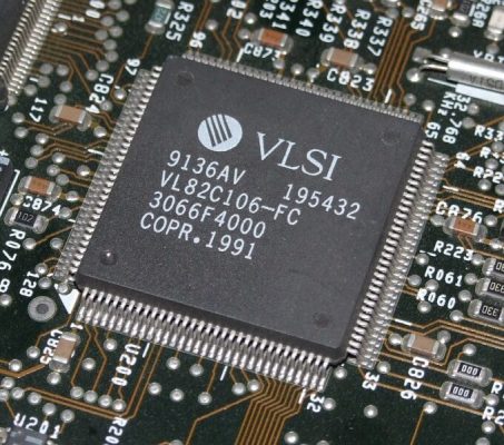
VLSI refers to Very Large Scale Integration and it’s the process of building an IC. IC means Integrated Circuits. Using VLSI, millions of MOS transistors can be implemented into a single chip. Starting in the 1970s, MOS chips integrated chips were widely adopted. Therefore, it enabled complex semiconductors and telecommunications.
In the last few decades, there has been exponential growth in the IC industry with computers offering advanced productivity and performance. Just as Tony Stark miniaturized arc reactor, the IC industry has miniaturized devices while maintaining functionality. The circuit density increases 40% every decade providing overall increased performance.
CMOS in VLSI
Till date, CMOS remains the most popular semiconductor. Complimentary Metal Oxide Semiconductor, is used to form IC. Computers, CPU, cell phones use CMOS technology. It is the most used MOFSET technology.
This technology uses P and N channel semiconductor devices. The major advantage of CMOS over NMOS and BIPOLAR technologies is that CMOS dissipates very little power. Therefore with no power dissipation, CMOS offers better performance.
But there are symptoms which when occur implied the CMOS battery has failed. For example, computer fails to maintain time and date. It may suddenly change to 1 AM January 1988. Other symptoms include, a continuous beep sound from the motherboard and difficulty in internet connectivity. Booting up become troublesome and the peripherals of the computer start to malfunction.
A brief history of VISL
General Microelectronics presented the main business MOS integrated circuit in 1964.[2] In the mid 1970s, MOS coordinated circuit innovation permitted the joining excess of 10,000 semiconductors in a solitary chip.[3] This readied the VLSI during the 1970s and 1980s, with a huge number of MOS semiconductors on a solitary chip (later many thousands, then, at that point, millions, and presently billions).
The main semiconductor chips held two semiconductors each. Resulting progresses added more semiconductors, and as an outcome, more individual capacities or frameworks were incorporated over the long haul. The originally incorporated circuits held a couple of gadgets, maybe upwards of ten diodes, semiconductors, resistors and capacitors, making it conceivable to create at least one rationale doors on a solitary gadget. Presently referred to reflectively as small scale integration(SSI), enhancements in procedure prompted gadgets with many rationale entryways, known as medium-scale integration (MSI). Further upgrades prompted large scale integration(LSI), for example frameworks with somewhere around 1,000 rationale entryways. Current innovation has moved far past this imprint and the present microchips have a huge number of doors and billions of individual semiconductors.
Moore’s Law
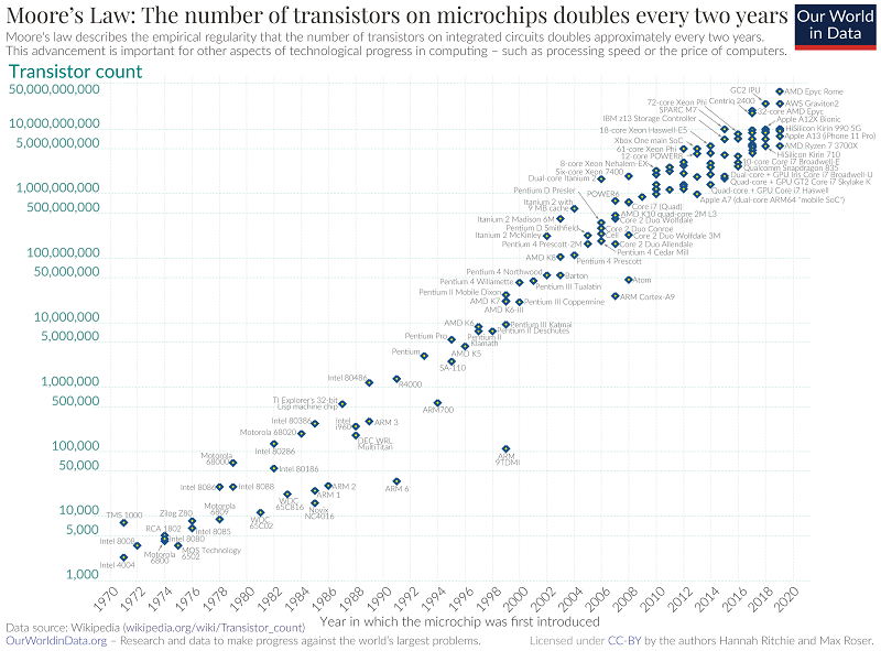
Gordon Moore was the co-founder of Intel. He, in 1965 predicted that the number of transistors will double every 18 to 24 months. He stated that the scaling of CMOS technology will lead to the shrinking of the size of transistors, even going in Nanoscale. Moore’s Law has since been the golden rule for the electronics industry and the stepping stone of innovation. Moore’s Law has transformed the computer industry by making it a pervasive necessity from being rare and costly.
Moore’s discovery has led to the miniaturization of VLSI chips with high integration, high performance and richer featured. A single large VLSI chip can now contain a billion transistors!
But we are moving towards a future where Moore’s Law will no longer be relevant. Physicist Michio Kaku says it’s already happening. Moore’s Law is said to break down in the coming decades. Kaku says Moore’s Law us already slowing down. Computers can’t keep up with the technology with standard silicon tech. Kaku says computers will evolve into chip like size in 3D. And in the late 21st century we can have quantum computers.
Advantages of VLSI
Below are the primary advantages of VLSI technology:
- Reduced size for circuits
- Increased cost-effectiveness for devices
- Operating speed performance increases
- Requires less power than discrete components
- Higher device reliability
- Requires less space and promotes miniaturization
Trends in VLSI Technology
ICs had a limited set of functions they could perform. But after the introduction of VLSI technology, they perform a lot more. An electronic circuit might consist of a CPU, ROM, RAM. VLSI lets IC designers add all of these into one chip.
The electronics industry has achieved remarkable growth over the last few decades. This is due to the rapid advances in large scale integration technologies and system design applications. With the advent of very large scale integration (VLSI) designs, the number of applications of integrated circuits (ICs) in high-performance computing, controls, telecommunications, image and video processing, and consumer electronics has been surging at a very quick pace.
Modern VLSI trends are gradually moving from vast to portable devices. In the last three years, significant increase in the productivity and performance of mobile processors was seen. The IC industry has constantly continued to make devices geometry smaller.
According to IRTS, the following changes in general trends can be expected:
- Greater increase in the number of transistors for processors and DRAM memory features.
- The lime widths of IC’s will relatively be shrunk to smaller sizes.
- Some growth in the chip dies sizes would be seen.
- Semiconductor fabrication practice will also be increasingly complex.
Difficulties in VLSI in the future
In the current and coming decades VLSI design – which currently enables us to build million-transistor chips will become Gigascale (GSI) design and Terascale Scale Integration (TSI) design, respectively. In this context, “gigascale” and “terascale” signifies more than one billion and one trillion devices per chip, respectively. The increase in integration levels is qualitatively different from past integration improvements of similar magnitudes. In particular, manufacturing defects will increase, devices will get less reliable, and new nanotechnologies will ensue. The signal and power management issues will be exacerbated. It is reasonable that new nanotechnologies will be used to complement or renovate CMOS. The future anticipates some of the unique system design challenges feigned by expected nanoscale CMOS and molecular electronics technologies.